
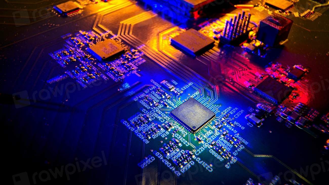
Inside $119B Terafab World’s Largest Building SHOCKED: The future of artificial intelligence, autonomous vehicles, humanoid robots, and advanced manufacturing depends on one critical resource: computing power. As AI systems become more sophisticated, companies need increasingly powerful processors, reliable semiconductor supplies, and manufacturing systems capable of producing chips at enormous scale.
According to the video “Inside $119B Terafab World’s Largest Building SHOCKED!” by TESLA CAR WORLD, Tesla and SpaceX are pursuing two major engineering directions that could reshape their long-term technology strategies: the proposed $119 billion Terafab semiconductor complex in Texas and a rare-earth-free electric motor associated with the Tesla Cybercab.
Together, these technologies illustrate a broader push toward manufacturing independence, supply-chain resilience, automation, and higher production efficiency.
The $119 Billion Terafab Semiconductor Mega-Factory
Tesla’s ambitions extend far beyond electric vehicles. The company’s future plans involve autonomous transportation, Optimus humanoid robots, AI computing, energy systems, and advanced manufacturing. SpaceX similarly requires sophisticated electronics for satellites, spacecraft, and future orbital infrastructure.
All of these technologies depend heavily on semiconductors.
Why Tesla Wants Greater Semiconductor Independence
Modern semiconductor production is highly distributed across the world. Different stages can involve silicon materials, wafer fabrication, memory production, advanced packaging, and testing in separate locations.
This fragmented structure can create vulnerabilities. If a critical manufacturing region experiences geopolitical disruption, transportation problems, natural disasters, or production shortages, downstream manufacturers may face delays.
The Terafab concept is presented as an attempt to address this challenge by bringing a much larger portion of the semiconductor ecosystem together in Grimes County, Texas.
Instead of relying entirely on a globally distributed chain, the proposed facility would integrate multiple stages of production within one enormous industrial complex.
A Factory Designed at Extraordinary Scale
The reported numbers associated with Terafab are enormous.
The project is described as potentially covering approximately 100 million square feet, or roughly 9.3 million square meters. That would make the proposed complex dramatically larger than conventional semiconductor manufacturing facilities.
The reported investment target is approximately $119 billion, with an initial phase estimated at around $16.3 billion.
If the proposed production targets are achieved, the complex could eventually aim for approximately one million wafers per month.
That would represent an extraordinary manufacturing operation, particularly if the facility incorporates multiple semiconductor technologies rather than focusing on a single chip family.
One Roof for the Semiconductor Supply Chain
The central concept behind Terafab is vertical integration.
The proposed ecosystem could include:
- Advanced logic fabrication
- AI processor manufacturing
- Memory production
- Advanced semiconductor packaging
- Chip testing
- Specialized space-grade electronics
- Large-scale power infrastructure
- Water recycling and industrial support systems
For Tesla, such an ecosystem could theoretically support processors used by autonomous vehicles and Optimus robots. For SpaceX, specialized electronics could support satellites and other space systems.
The concept therefore goes beyond simply building another chip factory. It represents a vision for a highly integrated technology-manufacturing campus.
Terafab’s Massive Power Requirements
Semiconductor manufacturing requires enormous amounts of reliable electricity. Advanced fabrication facilities cannot simply depend on an ordinary industrial power connection.
The Terafab concept described in the video includes a dedicated power ecosystem potentially involving more than 40 natural-gas turbines, generating close to 2 gigawatts of power, alongside battery storage and other infrastructure.
Water management is another major consideration. Semiconductor manufacturing requires highly controlled water systems, making water recycling an important component of any large-scale fabrication campus.
These supporting systems could be nearly as important as the fabrication equipment itself because continuous chip production requires extremely stable environmental conditions.
The Free Electron Laser Concept
One of the more futuristic elements discussed in the video is a potential Free Electron Laser (FEL).
The concept is associated with next-generation lithography and could theoretically provide new approaches to producing extremely small semiconductor features.
However, it is important to distinguish conceptual or proposed technology from commercially demonstrated production technology. The presence of an FEL in conceptual Terafab discussions does not by itself establish that such a system will be deployed or that it will replace existing lithography platforms.
Nevertheless, the idea demonstrates the scale of technological ambition associated with the project.
Tesla’s Rare-Earth-Free Cybercab Motor
The second major technology highlighted in the video is Tesla’s next-generation electric drive unit associated with the Cybercab.
Electric motors traditionally use permanent magnets containing rare-earth elements such as neodymium, praseodymium, dysprosium, and terbium.
These materials can provide strong magnetic performance but introduce additional supply-chain considerations.
Tesla’s proposed approach seeks to eliminate these rare-earth elements entirely.
Ferrite Magnets and Halbach Arrays
Instead of relying on rare-earth permanent magnets, the motor concept uses ferrite magnets combined with a Halbach array arrangement.
A Halbach array is a specialized magnetic configuration designed to concentrate magnetic flux on one side while reducing it on the other.
The engineering challenge is significant because ferrite magnets generally provide lower magnetic strength than high-performance rare-earth magnets.
The solution therefore requires optimization across several areas, including motor geometry, rotational speed, cooling, winding design, and magnetic-field management.
Smaller, Lighter and Highly Automated
According to the video’s claims, the Cybercab drive unit is approximately 18% smaller and 25% lighter than the previous design while maintaining the required performance characteristics.
The motor is also described as operating at extremely high rotational speeds, potentially reaching 15,000 to more than 20,000 RPM.
Higher rotational speed can contribute to greater power density, although it also creates engineering challenges involving heat, mechanical stress, bearings, lubrication, and durability.
Another important feature is the use of flat copper hairpin windings.
Why Hairpin Windings Matter
Traditional electric motors commonly use round copper wire. Hairpin designs instead use precisely shaped rectangular copper conductors.
This can increase the amount of copper packed into the stator slots.
The video describes a potential increase in slot-fill density from approximately 40% to around 70%. Better conductor utilization can help improve electrical performance and thermal management.
The manufacturing process is also designed for automation. The drive unit is described as having a potential sub-10-second production cycle, highlighting Tesla’s broader focus on designing products around high-volume manufacturing.
What These Two Technologies Have in Common
At first glance, a semiconductor mega-factory and an electric motor may appear unrelated.
But both technologies address the same strategic theme: reducing dependence on vulnerable external supply chains while increasing manufacturing efficiency.
Terafab focuses on semiconductors and computing infrastructure, while the Cybercab motor focuses on electric drivetrain technology and material independence.
For Tesla, these areas could become increasingly important as autonomous vehicles, robotics, AI systems, and automated factories expand.
The Bigger Manufacturing Vision
The proposed Terafab project represents an ambitious vision for vertically integrated semiconductor production, while the Cybercab motor demonstrates how Tesla can redesign individual components around material availability, efficiency, automation, and production speed.
Whether every proposed Terafab specification ultimately becomes reality remains to be demonstrated. Large semiconductor projects require enormous capital, specialized equipment, engineering expertise, utilities, workforce development, and years of execution.
Nevertheless, the underlying direction is significant.
The combination of AI computing, semiconductor manufacturing, electric motors, robotics, autonomous vehicles, and automated production points toward an industrial strategy in which technology companies increasingly control critical parts of their own supply chains.
If these concepts reach large-scale production, they could influence not only Tesla and SpaceX, but also the broader future of AI hardware, electric transportation, robotics, and advanced manufacturing.
FAQs
1. What is Tesla Terafab?
Tesla Terafab is a proposed large-scale semiconductor manufacturing complex intended to support technologies such as AI, autonomous driving, robotics, and advanced computing. The concept focuses on increasing semiconductor production and reducing dependence on fragmented global supply chains.
2. Where is the Terafab project planned?
The proposed Terafab complex is associated with Grimes County, Texas. The project is described as a massive industrial campus designed to integrate multiple stages of semiconductor production.
3. How much could Tesla Terafab cost?
The project has been described as requiring approximately $119 billion in investment across multiple phases. The initial phase has been discussed at roughly $16.3 billion.
4. How large could Terafab become?
The proposed facility is described as covering approximately 100 million square feet, or around 9.3 million square meters. That would make it an exceptionally large industrial complex.
5. How many wafers could Terafab produce?
The production target discussed in the video is approximately 1 million semiconductor wafers per month. Actual production capacity would depend on the technologies, fabrication processes, and facilities ultimately deployed.
6. Why does Tesla want its own semiconductor manufacturing?
Semiconductors are essential for Tesla’s AI systems, autonomous vehicles, robotics, and other technologies. Greater control over chip production could potentially reduce exposure to supply-chain disruptions and shortages.
7. What would Terafab manufacture?
The proposed ecosystem could include AI processors, advanced logic chips, memory, specialized space-grade electronics, semiconductor packaging, and testing. The exact final production mix would depend on how the project develops.
8. Could Terafab manufacture chips for Optimus?
The concept is intended to support Tesla’s broader AI and robotics ambitions, including Optimus humanoid robots. Advanced processors would be required for perception, inference, control, and other robotic functions.
9. Could SpaceX use chips produced at Terafab?
The proposed semiconductor ecosystem could potentially support space-grade electronics and satellite systems. Specialized radiation-resistant processors could be useful for demanding space environments.
10. How much power could Terafab require?
The video describes a potential dedicated power system approaching 2 gigawatts, including numerous natural-gas turbines, battery storage, and supporting infrastructure. Such power requirements reflect the energy-intensive nature of semiconductor manufacturing.
11. What is the Free Electron Laser mentioned in Terafab plans?
A Free Electron Laser (FEL) is a specialized technology that can generate highly controllable laser light. The video discusses it as a potential advanced lithography technology, although proposed concepts should not be confused with confirmed commercial deployment.
12. What is special about the Cybercab electric motor?
The Cybercab motor discussed in the video is designed around compactness, high power density, automation, and reduced dependence on rare-earth materials. It is described as a 163 kW electric motor.
13. Does the Cybercab motor use rare-earth elements?
According to the information presented in the video, the motor eliminates neodymium, praseodymium, dysprosium, and terbium. Instead, it uses ferrite magnets and a specialized magnetic arrangement.
14. What is a Halbach array?
A Halbach array is a magnetic arrangement that concentrates magnetic flux in a preferred direction while reducing it on the opposite side. In an electric motor, this configuration can help optimize magnetic performance when using different magnet materials.
15. Why does the Cybercab motor use hairpin windings?
Flat copper hairpin windings can allow more conductive material to occupy the stator slots compared with conventional round-wire windings. The video claims this can increase slot-fill density substantially while supporting improved electrical and thermal performance.
16. What do Terafab and the Cybercab motor have in common?
Both technologies reflect a broader emphasis on vertical integration, manufacturing efficiency, supply-chain resilience, and engineering optimization. Terafab focuses on semiconductor production and computing infrastructure, while the Cybercab motor focuses on electric drivetrain technology and reducing reliance on rare-earth materials.
Read More:
- Tesla Roadster is available for order once again following brief hold
- Why automakers keep turning down Elon Musk’s Tesla Full Self-Driving offer
- Did Tesla make the perfect car for families? Tesla Model Y L Full Review
- X changed how everyone gets paid, and this lawsuit shows why
- Starship Flight 14 Will Change the Space Industry Forever Begin Making Revenue