
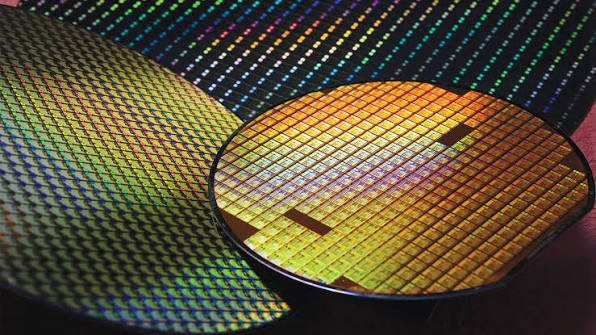
$119B Elon Musk’s Terafab Inside Is Impossible!: Modern AI and autonomous vehicles depend on enormous amounts of computing power. Companies such as TSMC and Samsung currently manufacture many of the world’s most advanced chips, but semiconductor capacity is becoming an increasingly important constraint.
For Musk’s ecosystem, the potential demand is enormous.
Future Tesla autonomous vehicles, Optimus humanoid robots, Starlink satellite constellations, and xAI supercomputers could require millions of advanced processors. If chip production cannot scale alongside these ambitions, hardware deployment could become the limiting factor.
Musk has argued that current global AI semiconductor production represents only a tiny fraction of the computing capacity that could eventually be required across his companies.
This creates what can be described as the silicon supply bottleneck: demand for AI compute could grow dramatically faster than semiconductor manufacturing capacity.
A dedicated megafab could theoretically give Musk greater control over that critical supply chain.
A Manufacturing Complex on an Unprecedented Scale
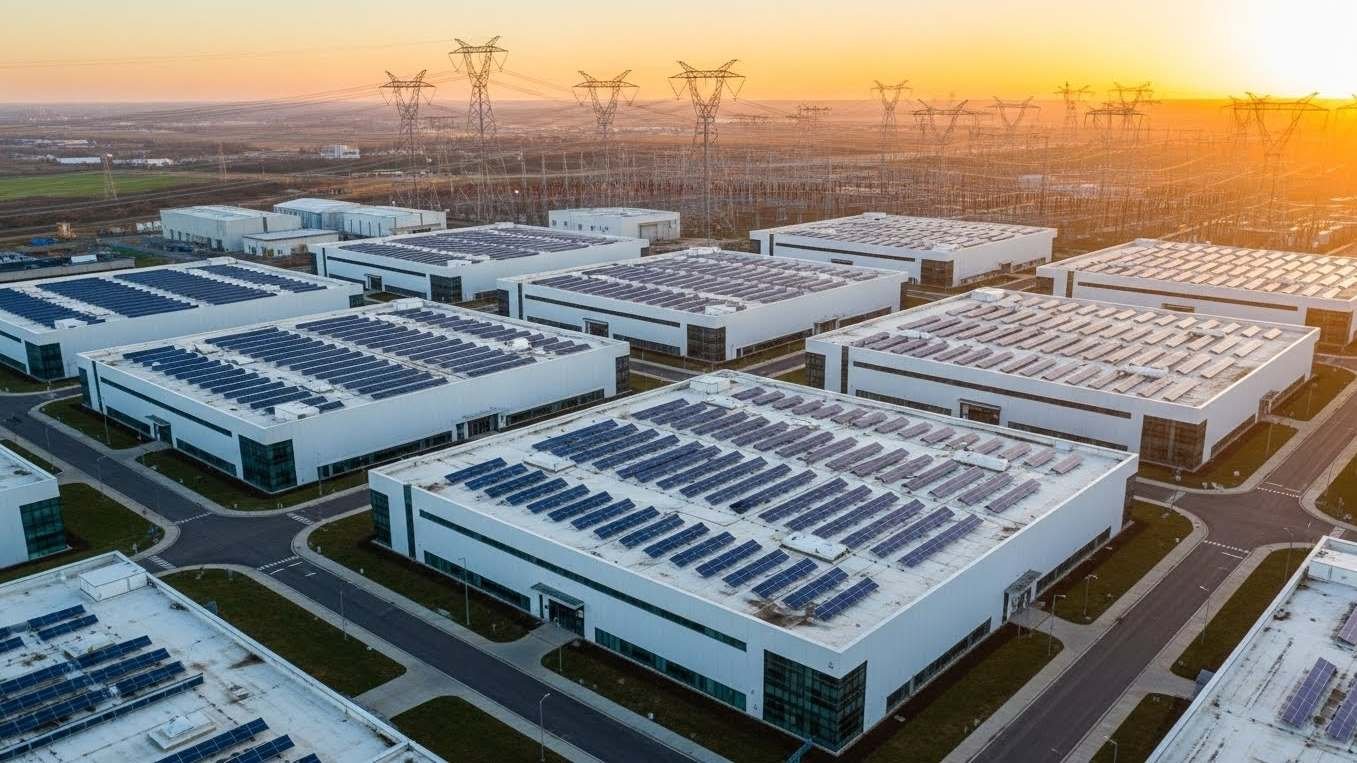
The proposed Terafab is described as a roughly 100 million-square-foot semiconductor manufacturing complex in Texas.
To understand the scale, that footprint would be approximately equivalent to 1,300 FIFA-standard soccer fields and around ten times the size of Tesla’s Texas Gigafactory.
The facility is envisioned with an eventual production capacity of up to 1 million silicon wafers per month.
The project could also create more than 3,000 direct high-tech and operational jobs, although the ultimate workforce and production schedule would depend on construction, technology development, and industrial execution.
The sheer size of the proposed facility is one reason the Terafab concept has attracted so much attention. Building a conventional semiconductor fab is already extraordinarily complex. Building one at this scale would require enormous quantities of electricity, water, specialized equipment, chemicals, precision machinery, and advanced logistics.
The Mystery of the Central Free Electron Laser
Why EUV Lithography Matters
One of the most fascinating elements of the proposed Terafab design is its unusual central architecture.
Advanced semiconductor manufacturing relies on extreme ultraviolet (EUV) lithography, a process that uses extremely short-wavelength light—around 13.5 nanometers—to print microscopic patterns onto semiconductor wafers.
Today’s EUV systems generally generate this light using powerful lasers that strike microscopic droplets of molten tin. The resulting plasma produces EUV radiation, which is then collected and directed through an intricate optical system.
Every EUV scanner therefore requires sophisticated light-generation infrastructure.
Could a Centralized FEL Change the Architecture?
The Terafab concept has raised speculation about a Free Electron Laser (FEL) serving as a centralized source of high-power EUV light.
Instead of each lithography machine having an individual light-generation system, a centralized accelerator could theoretically produce a powerful, precisely controlled beam that could be distributed among multiple lithography tools.
A free electron laser works by accelerating electrons to extremely high speeds and passing them through magnetic structures called undulators. This interaction generates highly controlled electromagnetic radiation.
If such an architecture could be engineered and integrated successfully for semiconductor manufacturing, it could potentially change how a gigantic fab distributes light generation, power, cooling, and maintenance infrastructure.
However, this remains one of the most technically challenging aspects of the Terafab concept. Turning a theoretical or experimental architecture into a reliable, high-volume commercial semiconductor process would be a monumental engineering challenge.
Terafab’s Dedicated Energy Strategy
Why Semiconductor Fabs Need Firm Power
A semiconductor fab cannot simply tolerate frequent power interruptions.
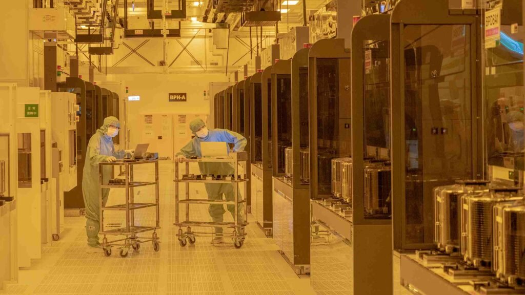
Advanced lithography and wafer-processing equipment operate with extremely tight tolerances. A significant interruption can potentially damage processes, disrupt production, and create enormous financial losses.
That makes reliable electricity just as important as chipmaking equipment.
The proposed Terafab energy architecture reportedly combines co-located natural gas power generation with large-scale Megapack battery storage.
The objective would be to create a supply of continuous or firm power, reducing dependence on an unstable external grid.
Battery storage could also provide rapid response during fluctuations, while on-site generation could supply sustained electricity when necessary.
This approach highlights a broader Musk strategy: controlling not only the products but also the infrastructure required to manufacture and operate them.
The Production-Ready Tesla Cybercab
While Terafab focuses on the semiconductor side of the equation, Tesla’s Cybercab represents the consumer-facing side of Musk’s autonomous transportation strategy.
The Cybercab is designed specifically as a robotaxi, rather than simply being a conventional Tesla adapted for autonomous driving.
A Vehicle Built Around Autonomy
One of the Cybercab’s most striking features is the absence of a traditional driver interface.
The vehicle is designed without a steering wheel or conventional pedals, reflecting Tesla’s goal of making autonomous operation the primary function rather than an optional feature.
Its aerodynamic design reportedly targets a drag coefficient below 0.20, helping improve energy efficiency.
Key dimensions include:
- Height: 55.4 inches
- Width: 69.0 inches
- Ground clearance: approximately 5.7–5.8 inches
- Step-in height: approximately 16.5 inches
- Cargo capacity: 20.2 cubic feet, or about 572 liters
The vehicle also uses upward-opening butterfly-style doors, giving passengers easier access in dense urban environments.
Cybercab Engineering and Battery Technology
Powertrain and Braking
The Cybercab is described as using a single front-mounted permanent-magnet motor producing approximately 219 horsepower.
Instead of a traditional hydraulic braking system, the architecture incorporates electronic brake-by-wire technology. This approach removes conventional physical hydraulic connections between the driver’s controls and braking hardware.
The Cybercab’s battery is equally important.
Tesla has developed a 48 kWh structural 4680 battery pack using dry-cathode cell technology. The pack is designed to contribute to the vehicle’s structural architecture while targeting long service life.
The estimated real-world range is around 300 miles, although actual range would vary according to driving conditions, weather, passenger load, speed, and autonomous operating patterns.
Tesla’s Unboxed Manufacturing Process
The Cybercab is also significant because of how Tesla intends to manufacture it.
Tesla’s Unboxed Manufacturing Process is designed to assemble major vehicle sections in parallel instead of relying entirely on a traditional sequential production line.
Front and rear assemblies, side structures, painted components, and structural battery modules can be prepared simultaneously before being integrated.
The potential advantages include a smaller manufacturing footprint, lower production complexity, faster assembly, and reduced costs.
Tesla has previously positioned the Cybercab toward an eventual purchase price around $30,000, although actual pricing and availability can depend on production scale and market conditions.
The Bigger Picture: Musk’s Vertical Integration Strategy
Terafab and Cybercab may appear to be completely different projects, but they share a common philosophy.
The Cybercab requires autonomous computing, cameras, batteries, motors, software, communications, and manufacturing capacity.
The Terafab would potentially provide part of the semiconductor infrastructure needed to support those systems.
Meanwhile, Starlink provides satellite connectivity, xAI develops artificial intelligence systems, and Optimus represents another major potential consumer of AI chips and autonomous computing.
This creates the possibility of an integrated technology ecosystem where chips, energy, AI, vehicles, robots, satellites, and manufacturing reinforce one another.
Final Thoughts
The proposed $119 billion Terafab is undoubtedly an extraordinary concept. Its enormous footprint, potential wafer output, centralized laser architecture, and dedicated energy infrastructure would make it one of the most ambitious semiconductor manufacturing projects ever envisioned.
The Tesla Cybercab, meanwhile, shows how Tesla is attempting to translate advances in AI and manufacturing into a purpose-built autonomous vehicle.
Whether every aspect of Terafab ultimately becomes reality remains an open question. Semiconductor manufacturing is among the world’s most technically demanding industries, and building a fab at this scale would involve enormous engineering and financial challenges.
But the underlying objective is clear: Musk wants to remove the infrastructure bottlenecks that could prevent his companies from scaling AI and autonomous systems.
If successful, the combination of massive semiconductor capacity, dedicated energy generation, autonomous vehicles, AI computing, robotics, and satellite connectivity could create an ecosystem unlike anything currently operating in the technology industry.
FAQs
1. What is Elon Musk’s Terafab?
Terafab is a proposed massive semiconductor manufacturing complex associated with Elon Musk’s broader plans for AI, robotics, autonomous vehicles, and computing infrastructure. The concept is intended to address potential semiconductor supply shortages as demand for advanced AI chips increases.
2. How much is the Terafab project expected to cost?
The proposed Terafab has been described as a $119 billion semiconductor megaproject. The enormous figure reflects the potential scale of the facility, advanced manufacturing equipment, energy infrastructure, and supporting systems required for a next-generation chip complex.
3. Where would Elon Musk’s Terafab be built?
The proposed Terafab is planned for Texas, continuing Musk’s growing manufacturing and technology presence in the state.
4. How large would the Terafab facility be?
The proposed complex could cover approximately 100 million square feet, making it dramatically larger than conventional semiconductor manufacturing facilities and several times larger than major industrial factories.
5. Why does Tesla need its own semiconductor factory?
Tesla’s future plans involve autonomous vehicles, humanoid robots, AI computing, and other high-performance systems, all of which require large quantities of advanced processors. A dedicated semiconductor facility could potentially reduce dependence on external chip manufacturers and improve supply-chain control.
6. What is the semiconductor bottleneck?
The semiconductor bottleneck refers to the possibility that global chip-manufacturing capacity may not grow quickly enough to satisfy future demand for AI processors and autonomous systems. For companies planning to deploy millions of intelligent machines, limited chip supply could become a major constraint.
7. How many wafers could Terafab produce?
The proposed Terafab has been described as having the potential to scale toward 1 million silicon wafers per month. Such output would represent an extraordinary manufacturing target and would require highly advanced production infrastructure.
8. What is EUV lithography?
Extreme ultraviolet (EUV) lithography is an advanced semiconductor manufacturing technology used to create extremely small patterns on silicon wafers. Modern EUV systems operate at a wavelength of approximately 13.5 nanometers, enabling manufacturers to produce increasingly sophisticated chips.
9. What is a Free Electron Laser (FEL)?
A Free Electron Laser is a type of light source that generates highly controlled electromagnetic radiation by accelerating electrons to extremely high speeds through magnetic structures. The Terafab concept has sparked interest because a centralized FEL could potentially serve multiple lithography systems.
10. Why would Terafab need its own power plants?
A semiconductor factory requires extremely stable and reliable electricity. Even significant power disruptions can interfere with sensitive manufacturing processes. The proposed Terafab energy strategy reportedly includes on-site natural gas generation and large-scale battery storage to provide firm power.
11. What is the Tesla Cybercab?
The Tesla Cybercab is Tesla’s purpose-built autonomous robotaxi. Unlike a conventional Tesla adapted for self-driving, the Cybercab has been designed around autonomous transportation, with a simplified interior and no traditional steering wheel or pedals.
12. How much range does the Cybercab have?
The Cybercab has been associated with an estimated real-world range of around 300 miles. Actual range can vary depending on weather, speed, terrain, passenger load, and other operating conditions.
13. How powerful is the Tesla Cybercab?
The Cybercab is described as using a single front-mounted permanent-magnet motor producing approximately 219 horsepower.
14. What battery does the Cybercab use?
The Cybercab is described as using a 48 kWh structural 4680 battery pack featuring dry-cathode cell technology. Its structural design is intended to integrate the battery into the vehicle’s overall architecture while supporting long-term durability.
15. What is Tesla’s Unboxed Manufacturing Process?
Tesla’s Unboxed Manufacturing Process is an approach that aims to assemble major vehicle sections in parallel rather than following a traditional sequential production line. The strategy could help reduce factory footprint, manufacturing complexity, and production costs.
16. How are Terafab and Cybercab connected?
Terafab and Cybercab represent different parts of a broader vertical-integration strategy. The Cybercab requires AI processors, batteries, software, connectivity, and manufacturing capacity, while Terafab is intended to address the semiconductor side of that ecosystem. Together with Optimus, Starlink, and AI computing infrastructure, these projects illustrate Musk’s ambition to build an interconnected technology and manufacturing ecosystem.
Read More:
- The Real Reason SpaceX Chose Louisiana
- Tesla Full Self-Driving will now overtake manual driving to avoid disaster
- Tesla Robotaxi will be a 24/7 service: here’s when
- SpaceX Falcon 9’s Retirement Begins Totally Shocked the Industry, Why? Can Starship Replace?
- NEW TESLA MODEL 2 IS REAL! The Cyber Cab Trick That Could Destroy BYD, Ford & GM in 2026
1 thought on “$119B Elon Musk’s Terafab Inside Is Impossible!”