
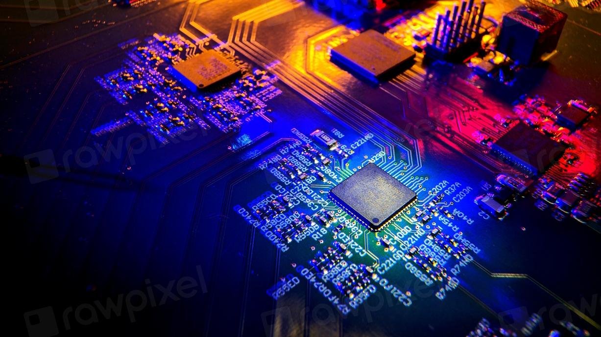
Elon Musk’s New Update On $119B Terafab, Biggest Building On Earth: The global artificial intelligence (AI) race is entering a new phase where computing power is becoming just as important as software innovation. From autonomous vehicles and humanoid robots to satellites and advanced data centers, the demand for powerful, efficient semiconductors is growing at an unprecedented rate. But producing those chips at scale is one of the most difficult industrial challenges in the world.
According to the Terafab concept outlined by Elon Musk, the answer could be a massive semiconductor manufacturing ecosystem in Grimes County, Texas, backed by Tesla and SpaceX.
Known as Terafab, the proposed mega-facility is designed to integrate several critical stages of semiconductor production into one enormous industrial complex. With a reported footprint of more than 100 million square feet and a potential investment of up to $119 billion, the project represents an extraordinarily ambitious attempt to reshape the semiconductor supply chain.
Why Elon Musk Wants a Massive Chip Factory
Modern semiconductor manufacturing depends on an extremely fragmented international supply chain. Different countries specialize in different stages of production.
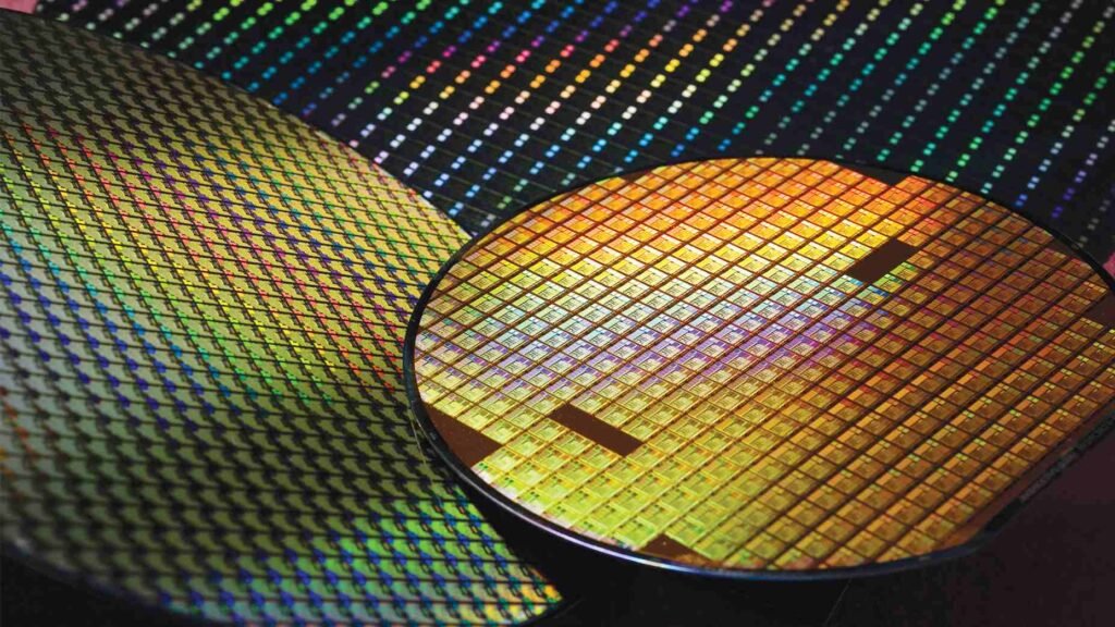
Raw silicon can originate in Japan, advanced logic wafers are heavily associated with Taiwan, high-bandwidth memory (HBM) is strongly concentrated in South Korea, while advanced chip packaging and testing take place across multiple global facilities.
This specialization has created an efficient system, but it also creates vulnerabilities.
If a major supplier experiences a shortage, geopolitical disruption, transportation problem, or manufacturing failure, the impact can spread throughout the entire technology industry.
For companies developing AI systems, autonomous vehicles, humanoid robots, and spacecraft, waiting for chips from multiple suppliers can become a significant limitation.
Terafab is designed around a different philosophy: vertical integration.
From Fragmented Supply Chains to One Integrated Facility
The traditional semiconductor supply chain can look something like this:
Raw Silicon → Logic Fabrication → HBM Memory → Advanced Packaging → Testing
Terafab’s proposed model would bring many of these critical processes together under one massive industrial ecosystem:
Logic Chips + HBM Memory + Packaging + Testing = Integrated Semiconductor Production
The goal is to reduce dependence on external manufacturing bottlenecks and give Tesla and SpaceX greater control over their future computing requirements.
Terafab’s 100 Million Square Foot Scale
One of the most extraordinary aspects of the proposed project is its sheer physical size.
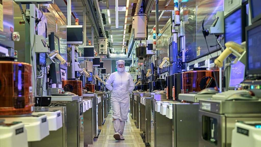
At more than 100 million square feet, Terafab would be comparable to a small industrial city rather than a conventional semiconductor factory. The enormous footprint would provide space for manufacturing facilities, cleanrooms, energy infrastructure, water systems, logistics, research operations, and advanced semiconductor equipment.
Building a semiconductor facility on this scale would require enormous amounts of electricity, water, specialized machinery, and engineering expertise.
The facility would also need to maintain exceptionally controlled environmental conditions because semiconductor manufacturing operates at microscopic scales.
A Gigawatt-Scale Power Requirement
Semiconductor fabs are among the world’s most demanding industrial facilities when it comes to electricity.
Even a short interruption or significant fluctuation in power can potentially damage sensitive manufacturing processes and result in substantial production losses.
The Terafab concept therefore includes a dedicated on-site power generation system, reportedly involving more than 40 natural-gas turbines with a combined capacity approaching 2 gigawatts.
Battery energy storage systems could provide additional stability and backup capacity.
This approach would allow the facility to operate with greater control over its electricity supply instead of depending entirely on the conventional grid.
Advanced Water Recycling
Electricity isn’t the only major requirement.
Semiconductor manufacturing also consumes enormous quantities of highly purified water. Ultra-Pure Water (UPW) is essential for cleaning semiconductor wafers throughout the manufacturing process.
A facility as large as Terafab would therefore require sophisticated water treatment and recycling systems.
The proposed infrastructure includes recycling systems connected with regional water resources, potentially allowing the facility to reuse substantial quantities of water and reduce its dependence on fresh municipal supplies.
The AI Chips Behind Tesla’s Future
A major objective of Terafab would be producing specialized chips designed around Tesla and SpaceX’s future requirements.
AI5 and AI6 Edge Inference Chips
Tesla’s future vehicles and robots require enormous amounts of computing power.
Instead of relying entirely on general-purpose processors, Tesla has been developing specialized hardware for AI inference, autonomous driving, and real-time decision-making.
Future generations such as AI5 and AI6 are intended to provide increasingly powerful processing for applications including autonomous vehicles and humanoid robots.
Running AI directly at the edge allows machines to process information locally, reducing dependence on remote cloud computing and potentially lowering latency.
For systems such as Optimus humanoid robots and autonomous vehicles, fast local processing could be particularly important.
Radiation-Hardened D3 Chips
Space presents a completely different semiconductor challenge.
Electronic components operating beyond Earth’s protective atmosphere face exposure to cosmic radiation, which can interfere with conventional electronics.
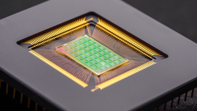
The proposed D3 chips are intended for radiation-resistant computing applications, potentially supporting future spacecraft, satellites, and orbital computing infrastructure.
This creates an interesting connection between Tesla’s terrestrial AI ambitions and SpaceX’s space-based technology ecosystem.
Terafab and the Future of EUV Lithography
One of the most technically ambitious elements associated with the Terafab concept involves Extreme Ultraviolet (EUV) lithography.
Modern advanced semiconductor manufacturing uses EUV light with a wavelength of approximately 13.5 nanometers to create extremely small patterns on silicon wafers.
Conventional EUV systems generate this light by firing powerful lasers at microscopic droplets of molten tin. The resulting plasma produces EUV radiation, which is then directed into the lithography system.
Musk has expressed interest in an alternative concept involving a Free Electron Laser (FEL).
Free Electron Laser Technology
An FEL uses high-energy electrons traveling through magnetic structures called undulators to generate powerful, coherent light.
Instead of relying on a separate light-generation system for every lithography scanner, a centralized accelerator-based system could theoretically generate EUV radiation and distribute it to multiple production systems.
If such an architecture could be developed and operated efficiently at industrial scale, it could potentially change the economics and infrastructure requirements of advanced lithography.
However, developing such technology for high-volume semiconductor manufacturing would be an enormous engineering challenge.
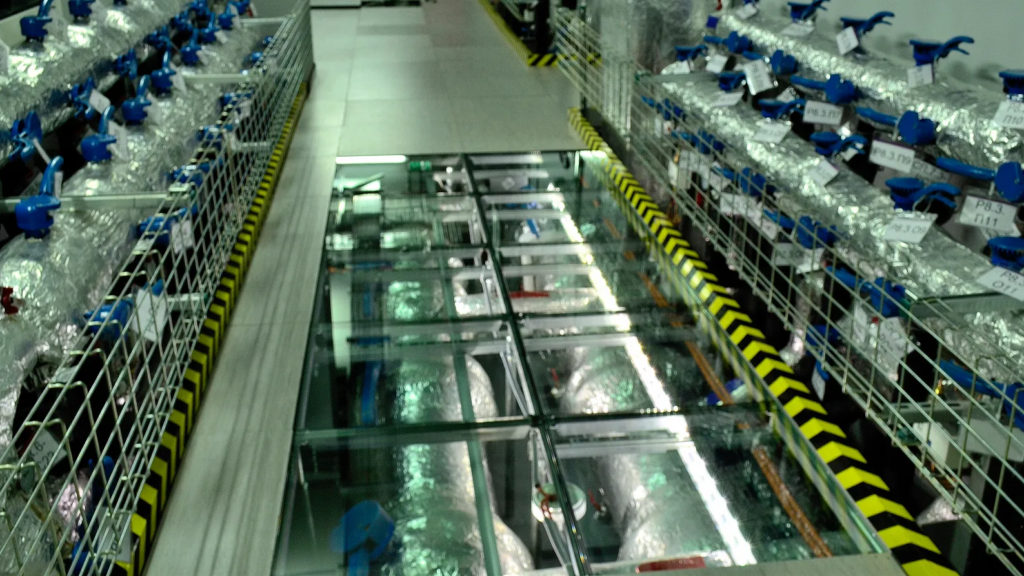
The Role of Intel and Manufacturing Expertise
Building a gigantic semiconductor facility is not simply a matter of investing money and installing machines.
The semiconductor industry depends heavily on decades of accumulated knowledge surrounding process engineering, yield optimization, materials science, contamination control, and manufacturing quality.
This is where experienced semiconductor manufacturers can play an important role.
The Terafab concept includes manufacturing expertise from established companies such as Intel, which could help with process-node transitions and high-volume manufacturing knowledge.
That expertise could be critical in transforming experimental semiconductor processes into reliable mass production.
The Biggest Opportunity—and the Biggest Risk
Terafab’s greatest advantage would be vertical integration.
Bringing logic manufacturing, memory, advanced packaging, testing, power generation, and supporting infrastructure into one ecosystem could dramatically reduce reliance on external suppliers.
For Tesla and SpaceX, that could provide greater control over the hardware needed for AI, robotics, autonomous transportation, and space exploration.
But concentration also creates risks.
Putting an enormous amount of production capacity in one geographic location creates a potential single-point-of-failure problem. Natural disasters, infrastructure failures, technical problems, or other disruptions could affect multiple stages of production simultaneously.
There is also the enormous challenge of reaching competitive manufacturing yields. Advanced semiconductor fabrication is one of the most technically complex manufacturing processes ever developed.
Conclusion: A New Vision for Semiconductor Manufacturing
Elon Musk’s proposed $119 billion Terafab represents an extraordinarily ambitious vision for the future of semiconductor production.
Rather than depending on a fragmented international network, the concept aims to combine logic fabrication, HBM memory, advanced packaging, testing, energy generation, water recycling, and advanced lithography infrastructure into one massive ecosystem.
If successfully developed, Terafab could support the growing computing requirements of Tesla’s autonomous vehicles, Optimus robots, and SpaceX’s future space systems while potentially reducing exposure to global semiconductor bottlenecks.
The project ultimately represents a much bigger idea than simply building another chip factory. It is a vision of creating an integrated industrial ecosystem capable of producing the computing infrastructure required for the next generation of artificial intelligence, robotics, and space technology.
FAQs
1. What is Elon Musk’s Terafab?
Terafab is a proposed mega-scale semiconductor manufacturing facility associated with Elon Musk, Tesla, and SpaceX. The concept is designed to integrate chip fabrication, memory production, advanced packaging, and testing into one large industrial ecosystem.
2. Where is Terafab supposed to be located?
The proposed Terafab facility is associated with Grimes County, Texas. Its planned scale would make it significantly larger than a conventional semiconductor manufacturing plant.
3. How much could Terafab cost?
The proposed project has been associated with a potential investment of up to $119 billion. Such an investment would cover semiconductor manufacturing infrastructure, power systems, water facilities, advanced equipment, and supporting industrial operations.
4. How large will Terafab be?
The Terafab concept calls for a facility spanning more than 100 million square feet, or approximately 9.3 million square meters. Its enormous footprint is intended to accommodate multiple semiconductor production and supporting operations.
5. Why does Elon Musk want to build Terafab?
The main objective is to reduce dependence on a fragmented global semiconductor supply chain. Bringing several manufacturing stages together could give Tesla and SpaceX greater control over chip production for AI, robotics, vehicles, and space applications.
6. What chips could Terafab produce?
The proposed facility could focus on specialized AI chips, including future generations such as AI5 and AI6, as well as specialized processors intended for robotics, autonomous vehicles, and space-related applications.
7. Could Terafab produce HBM memory?
The Terafab concept includes high-bandwidth memory (HBM) production as part of its integrated semiconductor ecosystem. HBM is particularly important for high-performance AI computing because it provides very high memory bandwidth.
8. What is the biggest advantage of Terafab?
One of its biggest potential advantages is vertical integration. Logic fabrication, memory, advanced packaging, and testing could operate within the same broader facility, potentially reducing delays caused by external suppliers.
9. Why is advanced packaging important for AI chips?
Modern AI processors often combine powerful logic with high-bandwidth memory using sophisticated 2.5D and 3D packaging technologies. Even when the semiconductor dies are available, insufficient packaging capacity can become a major production bottleneck.
10. How much electricity could Terafab require?
The proposed infrastructure includes more than 40 natural-gas turbines with a combined capacity approaching 2 gigawatts. Battery energy storage systems could also help provide additional power stability.
11. Why does Terafab need so much water?
Semiconductor manufacturing requires large quantities of Ultra-Pure Water (UPW) to clean silicon wafers during production. A facility on Terafab’s proposed scale would therefore require extensive water treatment, recycling, and purification infrastructure.
12. What is EUV lithography?
Extreme Ultraviolet (EUV) lithography is an advanced semiconductor manufacturing technology used to create extremely small patterns on silicon wafers. Modern EUV systems operate using light with a wavelength of approximately 13.5 nanometers.
13. What is the Free Electron Laser concept for Terafab?
A Free Electron Laser (FEL) generates intense light using high-energy electrons passing through magnetic structures. The Terafab concept has been associated with using a centralized accelerator-based EUV light source rather than relying exclusively on conventional EUV light-generation architectures.
14. What role could Intel play in Terafab?
Experienced semiconductor manufacturers such as Intel could provide valuable expertise in areas including process development, manufacturing, process-node transitions, and yield optimization. Semiconductor manufacturing requires decades of specialized operational knowledge.
15. What are the biggest risks facing Terafab?
The project would face substantial challenges, including construction costs, semiconductor yield optimization, advanced equipment requirements, power demands, water management, technology development, and supply-chain complexity. Concentrating multiple operations at one site could also create a single-point-of-failure risk.
16. Why is Terafab important for Tesla and SpaceX?
Terafab could potentially provide computing hardware for Tesla’s autonomous vehicles, Optimus humanoid robots, and future AI systems, while specialized semiconductor technology could support SpaceX’s satellites and space-based computing applications. Its broader goal is to create a more vertically integrated semiconductor ecosystem for future AI, robotics, and space technologies.
Read More:
- Tesla looks to expand into new Asian market, strengthening presence
- Elon Musk’s Boring Company has big plans for Las Vegas by year’s end
- Tesla Roadster unveiling is getting hyped up by Elon Musk
- Elon Musk gives his most telling Tesla-SpaceX merger conversation yet
- Tesla Semi 2027 New Version Officially Unveiled
1 thought on “Elon Musk’s New Update On $119B Terafab, Biggest Building On Earth”