
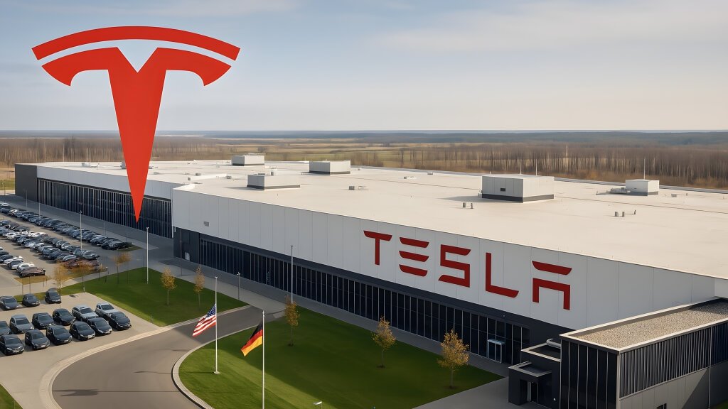
Amazing INSIDE Elon Musk’s World’s Biggest Terafab $119B: Elon Musk has built a reputation for taking on industries that once seemed impossible to disrupt. From electric vehicles through Tesla to reusable rockets and satellite internet with SpaceX, Musk’s companies have repeatedly pushed the boundaries of technology. Now, another ambitious project is attracting global attention: Terrafab, a proposed $119 billion semiconductor manufacturing mega-complex.
If realized, Terrafab could become one of the largest and most technologically ambitious chip-manufacturing projects ever conceived. The proposed facility is expected to cover an astonishing 100 million square feet and could eventually produce up to 1 million silicon wafers per month.
But Terrafab is designed to be much more than a traditional semiconductor factory. Its concept combines AI chip manufacturing, advanced lithography, robotics, logistics, energy generation, and industrial automation into a self-sustaining technology ecosystem.
What Is Elon Musk’s $119 Billion Terrafab?
Terrafab is envisioned as a massive semiconductor manufacturing complex in Texas, designed to address one of the biggest challenges facing Musk’s growing technology empire: the availability of advanced AI chips.
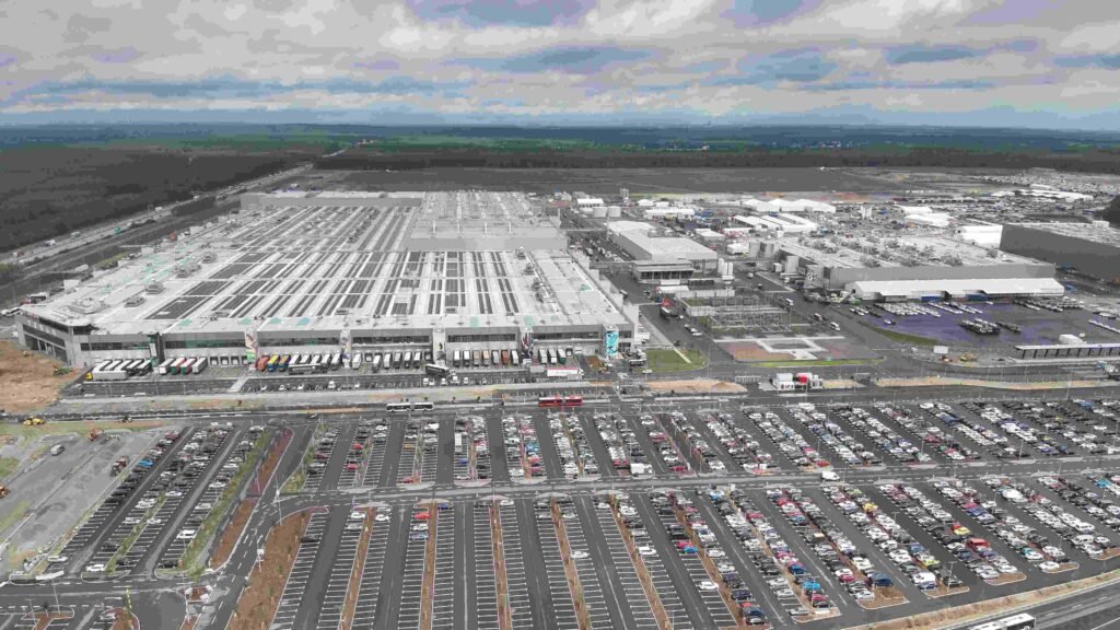
Companies and projects connected to Musk—including Tesla, SpaceX, Starlink, and xAI—are becoming increasingly dependent on enormous amounts of computing power.
Rather than depending entirely on outside semiconductor manufacturers, the Terrafab concept aims to bring a significant portion of chip production under Musk’s broader technology ecosystem.
The proposed $119 billion investment would make Terrafab an extraordinary bet on the future of artificial intelligence, autonomous vehicles, robotics, and space technology.
Why Does Elon Musk Need a Massive Chip Factory?
The Growing AI Chip Bottleneck
Modern AI systems require specialized processors capable of handling enormous quantities of data. As AI adoption accelerates, demand for advanced semiconductors is growing rapidly.
For Musk’s companies, this demand could become especially significant.
Tesla’s Cybercab requires powerful computing systems for autonomous driving. Cameras and other sensors must continuously process information about roads, pedestrians, vehicles, traffic signals, and unexpected hazards.
Tesla Optimus, Musk’s humanoid robot project, could require even more sophisticated computing. Robots need to understand their surroundings while simultaneously managing balance, movement, vision, object recognition, and physical interactions.
Meanwhile, SpaceX and Starlink could increasingly use onboard computing for satellite communications, routing, navigation, and collision avoidance.
Then there is xAI, whose large language models require huge clusters of AI accelerators for training and inference.
This creates a fundamental problem: Musk’s companies may need more advanced chips than existing suppliers can reliably provide.
Terrafab is therefore being presented as a potential solution to this supply bottleneck.
A 100 Million Square-Foot Semiconductor City
The physical scale of Terrafab is perhaps its most astonishing feature.
The proposed complex would reportedly span approximately 100 million square feet, or around 9.3 million square meters.
To understand the scale, that would be roughly:
- 10 times larger than Tesla’s Gigafactory Texas
- Around 50 times the floor area of the Pentagon
- Comparable to approximately 1,300 FIFA-standard soccer fields
At this size, Terrafab would effectively operate like an industrial city rather than a conventional factory.
Internal Transportation and Logistics
Workers could not simply walk from one side of the facility to another. The enormous footprint would require dedicated internal transportation systems, automated logistics corridors, and localized supply chains.
The complex could incorporate advanced robotics and automated material-handling systems to move silicon wafers, chemicals, components, and equipment throughout the facility.
The project could also create thousands of specialized jobs, including semiconductor engineers, cleanroom technicians, equipment specialists, infrastructure operators, and automation experts.
The Mystery Inside Terrafab: Free Electron Laser EUV
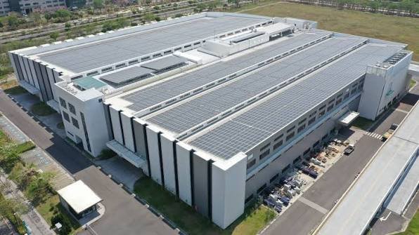
One of the most fascinating aspects of the Terrafab concept is its proposed central circular structure.
The giant ring has prompted speculation that it could house a Free Electron Laser (FEL) system designed to revolutionize extreme ultraviolet lithography.
How Conventional EUV Lithography Works
Today’s advanced semiconductor manufacturing relies heavily on Extreme Ultraviolet (EUV) lithography.
Conventional EUV systems generate 13.5-nanometer light by firing powerful lasers at microscopic droplets of molten tin. The resulting plasma produces EUV radiation, which is then carefully directed through extremely sophisticated optical systems.
This technology is extraordinarily complex and expensive.
How Free Electron Laser Technology Could Change Chipmaking
A Free Electron Laser works differently.
Instead of relying on tin plasma, electrons are accelerated to extremely high speeds through a magnetic structure called an undulator. Their movement can generate an intense, tunable beam of light.
In the Terrafab concept, a centralized FEL could potentially provide EUV radiation to multiple lithography areas.
That could represent a fundamentally different approach to fab architecture.
Instead of having a separate light source integrated into every individual lithography machine, a centralized system could theoretically distribute EUV capability across multiple scanner bays.
However, it is important to note that this remains a highly ambitious concept, and the practical engineering, reliability, beam-delivery, and manufacturing challenges would be enormous.
Can Musk Close the Semiconductor Expertise Gap?
Why Chip Manufacturing Is So Difficult
Building a semiconductor fab is fundamentally different from building an automobile factory.
Modern chip manufacturing requires atomic-level precision, ultra-clean environments, advanced chemicals, sophisticated equipment, and extremely strict process controls.
A tiny particle, vibration, temperature change, or manufacturing error can potentially damage an enormous number of wafers.
This is where Terrafab faces one of its biggest challenges: semiconductor manufacturing expertise.
Reports surrounding the project have pointed to experienced semiconductor executives and engineers, including leadership with deep Intel manufacturing experience.
Combining veteran chip-industry knowledge with Tesla’s automation capabilities and SpaceX’s rapid engineering culture could give Terrafab a stronger chance of overcoming the traditional startup learning curve.
Still, achieving consistently high semiconductor yields would remain one of the project’s greatest challenges.
The Massive Energy Challenge
A facility measuring 100 million square feet and operating continuously would require an enormous and highly reliable electricity supply.
Semiconductor factories cannot simply tolerate frequent power interruptions. A sudden electrical disturbance could interrupt sensitive manufacturing processes and potentially destroy valuable wafer runs.
Terrafab’s Proposed Energy Strategy
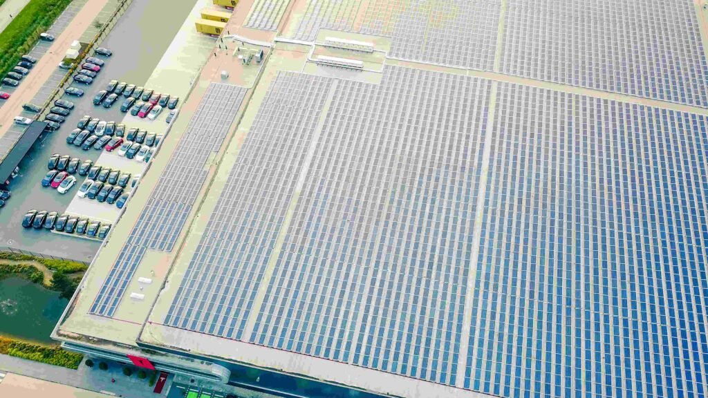
The concept reportedly includes dedicated islanded power infrastructure located near the semiconductor complex.
Potential components could include:
- Natural gas power generation for reliable firm electricity
- Tesla Megapack batteries for energy storage and rapid response
- Renewable or grid electricity where practical
- Battery systems to stabilize sudden changes in electrical demand
This combination could allow Terrafab to operate independently from some of the limitations of the wider Texas power grid.
The energy system would be almost as important as the semiconductor manufacturing equipment itself.
Could Terrafab Change the Global Chip Industry?
If Terrafab becomes a functioning semiconductor manufacturing operation at the proposed scale, its impact could extend far beyond Tesla and xAI.
The project would potentially challenge established semiconductor giants such as TSMC, Samsung, and Intel, while also creating a new vertically integrated model for AI hardware.
Instead of designing chips in one organization, manufacturing them through an external foundry, powering AI data centers separately, and developing robotics elsewhere, Musk’s ecosystem could potentially connect many of these activities together.
That would create a powerful form of vertical integration.
However, the gap between an ambitious concept and a successful semiconductor fab is enormous. Construction costs, equipment availability, manufacturing yields, regulatory requirements, energy infrastructure, supply chains, and workforce development would all have to align.
Conclusion: Is Terrafab the Future of AI Chip Manufacturing?
Elon Musk’s proposed $119 billion Terrafab represents one of the boldest visions for semiconductor manufacturing.
Its proposed 100-million-square-foot footprint, potential 1-million-wafer-per-month capacity, centralized Free Electron Laser EUV concept, advanced automation, and dedicated energy infrastructure would make it dramatically different from an ordinary chip factory.
The underlying motivation is straightforward: AI needs chips, and Musk’s companies are expected to need an extraordinary number of them.
Whether Terrafab ultimately becomes a real-world semiconductor powerhouse or remains an ambitious vision, the project highlights an increasingly important reality of the AI era: access to advanced computing hardware can be just as strategically important as the software running on it.
If Musk succeeds, Terrafab could do more than supply chips for Tesla, SpaceX, and xAI. It could introduce a radically different model for how the world’s most advanced AI hardware is designed, manufactured, powered, and deployed.
FAQs
1. What is Elon Musk’s Terrafab?
Terrafab is a proposed massive semiconductor manufacturing complex associated with Elon Musk’s technology ambitions. The concept is designed to produce advanced chips at enormous scale for applications including artificial intelligence, autonomous vehicles, robotics, and space technology.
2. How much will Elon Musk’s Terrafab cost?
The proposed Terrafab project is estimated at around $119 billion, making it one of the most ambitious semiconductor manufacturing investments ever proposed.
3. Where will Terrafab be located?
The proposed Terrafab complex is associated with Texas, where Musk already operates major facilities connected to Tesla and SpaceX.
4. How big will Terrafab be?
Terrafab is envisioned to cover approximately 100 million square feet, making it vastly larger than a conventional semiconductor factory and comparable in scale to an entire industrial city.
5. How many chips could Terrafab produce?
The concept reportedly targets production of up to 1 million silicon wafers per month. Actual production capacity would depend on the final design, manufacturing technology, equipment, and operational performance.
6. Why does Elon Musk want to build Terrafab?
The primary motivation is the growing shortage of advanced AI chips. Tesla, SpaceX, Starlink, and xAI all have increasingly large computing requirements, making reliable access to advanced semiconductors strategically important.
7. What companies could use chips made at Terrafab?
Potential users within Musk’s ecosystem could include Tesla, xAI, SpaceX, and Starlink. Chips could support autonomous vehicles, humanoid robots, AI models, satellites, and other advanced technologies.
8. What is Free Electron Laser EUV technology?
Free Electron Laser (FEL) EUV technology is a proposed alternative approach to generating extreme ultraviolet light for semiconductor lithography. Instead of producing EUV through conventional laser-generated tin plasma, an FEL uses accelerated electrons and magnetic structures to generate a powerful light beam.
9. Why is EUV lithography important?
EUV lithography is critical for manufacturing some of the world’s most advanced semiconductor chips. It allows manufacturers to create extremely tiny and complex features on silicon wafers, enabling more powerful and efficient processors.
10. Could Terrafab replace TSMC?
Terrafab is not currently positioned as a guaranteed replacement for TSMC. Building an advanced semiconductor foundry at this scale would involve enormous technical, financial, and operational challenges. If successful, however, it could become a significant competitor in advanced chip manufacturing.
11. How is Terrafab different from a normal chip factory?
Terrafab is envisioned as more than a traditional semiconductor fab. Its proposed design combines chip manufacturing with advanced lithography, automation, logistics, energy infrastructure, and potentially other industrial operations within one enormous complex.
12. How much energy would Terrafab require?
A 100-million-square-foot semiconductor complex operating around the clock would require an exceptionally large and stable power supply. The concept reportedly includes dedicated power generation and large-scale battery storage to provide reliable electricity.
13. Will Tesla Megapacks be used at Terrafab?
The proposed energy strategy includes the potential use of Tesla Megapack battery systems. Large-scale batteries could help manage demand spikes, stabilize electricity supply, and provide backup power for critical operations.
14. How many jobs could Terrafab create?
The project has been associated with the potential creation of thousands of specialized jobs, including semiconductor engineers, cleanroom technicians, equipment specialists, automation experts, and infrastructure workers.
15. What are the biggest challenges facing Terrafab?
The biggest challenges include enormous construction costs, semiconductor manufacturing expertise, equipment availability, energy requirements, supply-chain management, cleanroom technology, manufacturing yields, and the complexity of advanced lithography.
16. Could Terrafab change the global semiconductor industry?
If Terrafab is successfully built and achieves its proposed production goals, it could significantly influence the global semiconductor industry. Its combination of massive scale, AI-focused chip production, advanced lithography, automation, and dedicated energy infrastructure could create a new model for vertically integrated semiconductor manufacturing.
Read More:
- Tesla Cybertruck windshield protection just got cheaper
- Tesla surges Robotaxi fleet ahead of Cybercab launch event
- SpaceX would not exist if this crucial early launch failed, Musk says
- Tesla Cybercab Event: what to expect from Austin
- Starship Flight 14 to become the Biggest Leap ever: Unlike any others
1 thought on “Amazing INSIDE Elon Musk’s World’s Biggest Terafab $119B”